
1. Background of Pin Configuration Differentiation
The emergence of 6PIN, 16PIN, and 24PIN Type-C connectors stems from diversified application requirements and cost optimization strategies:
1.1 Application-Specific Tiering
24PIN (Flagship Tier):
Full support for USB4/Thunderbolt 4 (40Gbps), 100W PD fast charging, and Alt Mode video output.
16PIN (Mid-Range Tier):
Maintains USB3.2 Gen2 (10Gbps) and 60W power delivery.
6PIN (Entry-Level Tier):
Dedicated to USB2.0 (480Mbps) and 15W power applications.
1.2 Cost Optimization
Each additional high-speed differential pair (TX/RX) increases material costs by 12%, while pin reduction achieves 30-50% cost savings.
1.3 Mechanical Constraints
Wearable devices (e.g., TWS earphones) require ultra-compact connectors ≤2.5mm thickness (6PIN solution).
2. Technical Implementation of Pin Reduction
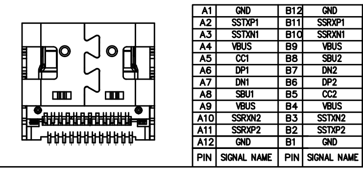
2.1 24PIN Architecture (Full-Featured)
4× High-Speed Differential Pairs (8 pins)
2× Sideband Use (SBU) Channels (2 pins)
2× Configuration Channels (CC1/CC2) (2 pins)
4× Power Delivery Paths (VBUS/GND) (8 pins)
2× Auxiliary Signal Groups (4 pins)
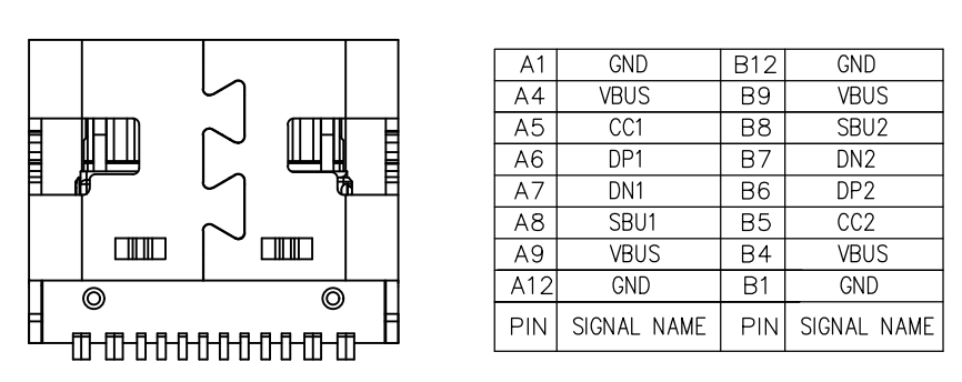
2.2 16PIN Optimization (Balanced Design)
Preserves 2× High-Speed Differential Pairs (4 pins)
Eliminates SBU channels
Consolidates VBUS power paths (3→2 groups)
Streamlines auxiliary signals (retains USB2.0 D+/D-)
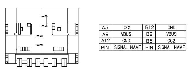
2.3 6PIN Minimalist Design (Basic Functionality)
Single USB2.0 Data Pair (2 pins)
Dual CC Channels (2 pins)
Essential Power Delivery (VBUS+GND)
3. Reversible Plugging Implementation
3.1 Topological Symmetry
24PIN: Mirror-symmetric pin layout (12 pins per orientation)
Reduced-Pin Solutions:
6PIN: CC1/CC2 positioned on central symmetry axis
16PIN: Maintains cross-coupled RX/TX differential pairs
3.2 Dynamic Signal Routing
CC Channel Arbitration: Real-time orientation detection via CC pin voltage thresholds
Path Switching Mechanisms:
6PIN: PHY-level signal inversion triggered by CC logic
16PIN: High-speed signal rerouting via crosspoint switches
3.3 Electrical Compliance
Contact impedance maintained at <50mΩ across all tiers
Impedance matching: 90Ω±10% for high-speed signal integrity
4. Selection Guidelines
| Parameter | 6PIN Solution | 16PIN Solution | 24PIN Solution |
|---|---|---|---|
| Data Rate | USB2.0 (480Mbps) | USB3.2 Gen2 (10Gbps) | USB4/Thunderbolt4 (40Gbps) |
| Power Delivery | 15W (5V@3A) | 60W (20V@3A) | 100W (48V@2.1A) |
| Target Applications | Wearables (TWS/IoT) | Tablets/Power Banks | Premium Laptops/Smartphones |
| Unit Cost | $0.12–0.18/pc | $0.25–0.35/pc | $0.45–0.65/pc |
| Manufacturing Spec | 0.8μm Au plating | 1μm Au plating | 30μm Au plating + laser welding |
5. Technology Roadmap
Adaptive Pin Multiplexing: FPGA-controlled dynamic pin function reallocation
Advanced Contact Materials: PdCo alloy replacing Au plating (10× durability improvement)
Embedded E-Marker: Chip-in-connector integration for real-time capability negotiation